Lowering Production Cost of “Big MEMS” Chip Technologies using Large Area Manufacturing Techniques
Veröffentlicht April 24, 2019 von Robert Andosca
Since the 1980s, microelectromechanical systems (MEMS) based devices have been manufactured primarily on round silicon substrates. This has been accomplished by primarily riding the coattails of the semiconductor integrated circuit chip industry, where Si substrate diameters have grown from less than 50 mm to 300 mm. As new, larger diameter fabrication equipment was needed, the previous generation tools (refurbished) were adopted by the MEMS industry at much lower price points.
Today, the SEMI industry has stalled at 300 mm; likewise, the MEMS industry is mired at 200 mm diameter. The issue is that many MEMS chip dimensions can be large, greater than 10 x 10 mm2 in area, and can have expensive wafer-level packaging utilized to protect its moving parts from inexpensive plastic molded packaging. When considering the $1 per mm2 rule of thumb for unyielded chip production cost, these “Big MEMS” chips are very difficult to fabricate cost effectively, inhibiting product market adoption.
Meanwhile, over the last two decades, flat panel display (FPD) technology requirements and manufacturing capabilities have become more complex. This includes increasing FPD resolution from today’s 4K to 8K and glass substrate size up to 3.1 x 3.1 m2, a.k.a. Gen 10 (G10) glass. To achieve these challenging levels, many manufacturing obstacles have been overcome, such as magnetron sputtering over large areas, including deposition thickness uniformity and optical property uniformity, the reduction of yield detractors, such as particles generated due to plasma arcing, and other process challenges.
What if the MEMS industry wasn’t restricted in substrate size, such as by utilizing G8 (2.1 x 2.4 m2) or older (smaller area) fabrication equipment? Then, the chip cost could dramatically decrease.
A “Big MEMS” Story
Prior to joining AE, I founded a company that utilized technology based on my Ph.D. research around the development of a piezoelectric MEMS (piezoMEMS) based vibration energy harvester (VEH). At the time, there was skepticism around whether we would be able to power a wireless sensor from such a small-scale power source, especially from low levels of vibration found in industrial environments. The size of the piezoMEMS VEH chip was ultimately as small as 1 x 1 x 0.3 cm3 with glass wafer-level-packaging, which is quite costly in low and even high manufacturing volumes. Small companies and even large corporations need deep pockets to bring a large-scale technology like this to market successfully.
So what happened next?
If you’ll be at this year’s SVC TechCon, join me during my May 2, 2019 keynote address. In it, I’ll share how we utilized an alternative piezoelectric material to power a wireless sensor, the impact that had on organizational research in the industry and how we then built upon that initial achievement to build a device that could survive inside a rotating tire, which enabled a tire pressure monitoring sensor system (TPMS). I’ll make my case around how I believe that Big MEMS chips are not being disruptively adopted by the market only because of their large size and resulting unit cost in low to even high-volume production levels. I’ll also advocate for the MEMS industry to begin utilizing LA manufacturing techniques to lower production cost. This is especially if the Internet of Things is truly going to be ubiquitous – some estimates are as high as 60 trillion sensors sold per year in 2035!
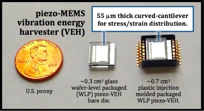
Figure 1. A single 1 cm2 piezo-MEMS VEH chip with WLP and plastic packaging COGS would be $70-100 each in low manufacturing volume produced on 200 mm diameter Si wafers. Power produced was 50 to 240 microWatts DC and could withstand up to 3,000 g drop-shock depending on resonant frequency.


