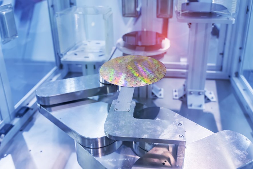
Spotlight on Inspection Solutions for Semiconductor Manufacturing
投稿 4月 30, 2019 によって Advanced Energy Editor
Chip manufacturers must find ways to continually improve device speed, reduce power consumption or reduce cost by moving to smaller nodes or more complex device geometries and structures. Inspection of these smaller nodes or more complex device structures and the added challenge of finding and identifying smaller “killer defects” requires the constant evolution of electron beam inspection tools.
Advanced inspection processes are now nearly universally deployed as part of the semiconductor device manufacturing process, the changes to smaller nodes, higher process step count and need for improved inspection speed require advancement in the high voltage power supplies that are critical for high performance inspection systems.
Advanced Energy offers a wide range of solutions for electron beam power supply applications that enable resolutions down to the one-nanometer level and beyond at voltages up to 60kV.
AE’s platform architecture, development expertise and application skills give you rapid access to customized solutions that help reduce technical program risks and ensure high performance. Our solutions provide ultra-low ripple with high stability and accuracy in an industry leading small volume package or rack mounted enclosure.
Learn more about our leading inspection solutions or talk to us about a custom requirement:
- EG353 Series: part of our E-beam power supply product line, EG353 is a 35 kV high voltage power supply designed for performance in your specific inspection applications.


