The Next Leap: Powering Plasma for the Angstrom Era
게시됨 2월 27, 2023 으로 Juergen Braun
Key Takeaways:
- Semiconductor manufacturing is advancing rapidly.
- Innovations in process equipment and power delivery technologies enable the creation of devices with atomic-scale dimensions.
- The industry is moving into the Angstrom Era, increasing the complexity of manufacturing processes.
- Exceptional agility and control in plasma power delivery systems are required.
- Advanced Energy is at the forefront of these innovations.
- They provide sophisticated RF plasma power solutions supporting advanced-node device development.
- New technologies offer precise control, high-speed responsiveness, and improved energy management.
- These advancements are essential for the next generation of semiconductor devices.
Semiconductor manufacturing pushes the boundaries of process innovation to the nearly impossible. Reaching a new device node is the culmination of vision, technology and partnership. These leaps forward are enabled by both possibility and capability. Often, the difference between the impossible and the next node comes down to process equipment innovations that open wholly new windows of performance and functionality.
Complexity is spiraling upwards. Higher feature densities are leading to 3D structures and novel transistor architectures with dimensions on the atomic scale, measured in angstroms (10-10 meters). Altogether, this demands unprecedented process control. Advanced-node devices drive ambitions for innovative process equipment — including extraordinary power-delivery technologies — to expand the limits of the possible.

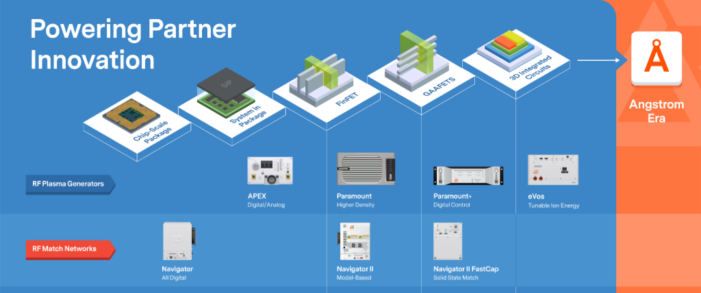
Radio frequency (RF) plasma power delivery systems have evolved to become highly sophisticated power control engines with ultrafast responsiveness — as different from earlier RF generators as a thoroughbred horse is from a donkey. High-speed, precise power delivery enables radical changes and industry inflections from chip-scale packaging through advanced front-end technologies including gate-all-around (GAA) transistors, backside power delivery (BPD) and the path to 3D DRAM.
As the semiconductor industry ventures into the Angstrom Era, plasma processes used to create these extraordinary devices require exceptional agility, complex pulsing sequences with near-instant tuning speeds, recipe-customizable control capabilities and, increasingly, direct control of the plasma ion energy that creates the devices.
Advanced Energy has been making impossible plasma processes possible for over 40 years. AE is once again leaping forward in plasma control by introducing transformational power delivery technologies to address the challenges of the Angstrom Era.
A History of Transformational Power-Delivery Solutions
The semiconductor industry has relied on AE’s plasma power innovations to jump from micron to submicron to nanometers and now to angstrom-dimension devices

These innovations have been instrumental in supporting leading-edge plasma processes starting from the chip-scale era when all-digital Navigator® technology provided three to five times the match speed and unsurpassed RF metrology compared to competing products. The sophistication of AE power delivery and match technology grew across the next chip design nodes, providing increasing precision, power density, performance features such as pulsing, as well as faster response to abruptly changing plasma conditions. Advanced Energy’s eVoS™ platform is an example of the kind of revolutionary power technology capabilities that change what’s possible in plasma processing with its direct ion energy control. And there’s more to come.
Leaping into the Angstrom Era
Process recipes are more complex than ever, with multiple steps as short as one second transitioning through very different plasma conditions — often without turning off power to the plasma. Nimble, reproducible, repeatable RF plasma power delivery is vital to manage the extreme swings in plasma impedance caused by frequent, abrupt and profound changes in gas flow, chemistry, pressure and power. In the most advanced deposition and etch processes, critical aspects include precise control of target-species energy and repeatability from wafer to wafer in highly non-linear plasma environments.
AE addresses these challenges with a leap ahead in plasma power control, providing the agility, stability and speed required to drive Angstrom-Era semiconductor applications. This new, forward-looking technology provides critical performance:
- Speed of control within pulse profiles
- Power overhead for reliable ignition
- Waveform customization and control
- Ion energy management via direct plasma sheath voltage control
- Interconnected, coordinated operation of all power delivery components on complex plasma wafer processing equipment
- IoT ecosystem: High-resolution, high-bandwidth data access and sophisticated analytics
Transcending the Impossible: Powering the Future
From its inception, the semiconductor industry has constantly pushed the physical limits of device dimensions, densities and speed. Continuing the march from nanometer to angstrom device dimensions will be a truly remarkable milestone. Evolutionary and revolutionary advances in process power will provide the drumbeat bringing this vision to fruition. Those at the forefront of plasma power delivery technology will be the primary enablers as the industry draws closer to once-impossible dimensions.
Preview AE’s new, transformational power delivery technology, which will be available this summer.


.png?resizemode=force&maxsidesize=884)